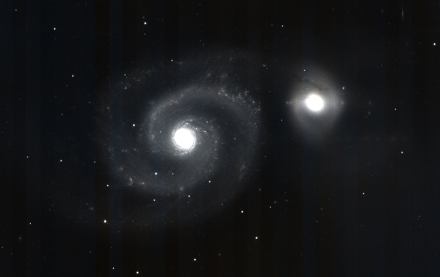
MAUNA KEA, Hawaii: The University of Hawaii’s Institute for Astronomy released the remarkable first infrared astronomy image on Thursday, which was taken by its 2.2-meter telescope on Mauna Kea with new 16-megapixel HAWAII 4RG-15 image sensor.


The field observed is 4096 pixels square and half the diameter of the moon. It is centered on the Whirlpool Galaxy (M51) in the constellation Canes Venatici, which is seen face-on. It is gravitationally interacting with the smaller companion galaxy. Spectacular star formation was triggered by this companion coming through the main disk of M51 about 500 million years ago and looping back through it in the last 50 to 100 million years. M51 can be seen through binoculars at a dark sky site and is familiar to amateur astronomers. Credit: UH Institute for Astronomy.
The University of Hawaii today released the first image obtained using its new 16-megapixel HAWAII 4RG-15 (H4RG-15) image sensor on the UH 2.2-meter (88-inch) telescope on Mauna Kea. This represents a significant step forward in astronomical infrared technology because it is the first time a sensor with anywhere near this many infrared pixels has been trained on the sky.
The image shows the Whirlpool Galaxy, a spiral galaxy 23 million light-years away. “The detail captured all across this extended infrared image really whets our appetite for getting these sensors into cameras at newer, much larger telescopes,” said Dr. Donald N. B. Hall of the UH Institute for Astronomy (IfA), who is principal investigator for the project. “The level of detail revealed by digitally zooming in anywhere in the 16-megapixel image is truly incredible.”
This sensor boasts 16 times the pixel count of an earlier sensor developed by the same team and installed on the Hubble Space Telescope during the astronauts’ last refurbishment mission. It also has four times the pixel count of the largest infrared sensors now in use at telescopes around the world.
While the 16-megapixel count is comparable to commercial imagers in today’s professional digital cameras, infrared sensors used for astronomy must also overcome two formidable technical challenges: The pixels must be sensitive to infrared colors, and they must be big enough to match the huge magnification of the image from a large telescope.
The H4RG-15 development, sponsored by the National Science Foundation, has overcome these challenges through an academic-industrial partnership that draws upon the combined expertise of the IfA, Teledyne Scientific and Imaging, GL Scientific and ON Semiconductor. This latest sensor is the culmination of a 20-year, $15-million effort that has developed five generations of increasingly larger and more powerful infrared sensors in the HAWAII series. The acronym stands for HgCdTe (mercury-cadmium-telluride) Astronomical Wide Area Infrared Imager.
To overcome the first of these major challenges—that the silicon used to fabricate visible imagers is blind to infrared light—infrared-sensitive crystals must be electrically connected to each of the 16 million pixels.
The second challenge, matching the image scale at the focus of a large telescope, means that the pixels must be huge—several hundred times that of the pixels in an iPhone, resulting in one of the largest silicon chips ever produced.

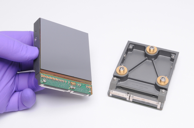
Front and back views of a 2-1/2 inch square H4RG-15 sensor mounted to its silicon carbide package. Teledyne Imaging Sensors, a world leader in creating infrared sensors, electrically connects infrared-sensitive crystals to each of the 16 million pixels by growing an alloy of mercury telluride and cadmium telluride onto a wafer that matches the readout, implanting the 16 million individual photodiodes and depositing a tiny (0.0002 inch) dot of indium at the center of each pixel. This infrared detector array is then precisely aligned with matching indium dots on the CMOS readout, and the two are clamped together with hundreds of pounds of force to complete the electrical connections, a process known as hybridization. Teledyne then mounts the hybrid sensor to a custom package produced by GL Scientific. Credit: GL Scientific.
The HAWAII-4RG-15 pushes the limits of current and foreseeable technology. Larger sensors can likely be constructed only by assembling mosaics of individual arrays, much like tiling a floor. With this technique, 64-megapixel and even gigapixel-class infrared sensors should be possible. GL Scientific, a Hawaii high-tech company founded by former IfA astronomer Dr. Gerard Luppino, is a world leader in mounting the sensors into packages and assembling these into mosaics.
The Infrared-Optical (IO) sensor development program is run out of the IfA’s Hilo facility on the Big Island of Hawaii, where Hall is located. “These detectors are vital to the long-term success of the James Webb Space Telescope and other upcoming space astronomy missions,” he commented. “They also greatly improve the infrared sensitivity of ground-based telescopes such as those on Mauna Kea today and are critical for the coming generation of 30-m-class telescopes, including the Thirty Meter Telescope planned for Mauna Kea.”
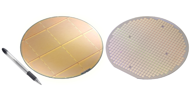
ABOVE: The four H4RG-15 readouts that can be fitted onto an eight–inch silicon wafer (shown left) contrast to the 400 plus typical computer chips in the wafer at right. (For comparison, an iPhone camera chip will easily fit within the pen.) The unprecedented yields for these very large scale silicon readouts can be attributed to the expertise and yield improvement efforts made by ON Semiconductor’s wafer fabrication teams driven by the Custom Foundry Business Unit. The achievement is a direct result of the company’s more than 35-year focus on meeting the technical needs of their military and aeronautics customers. The silicon wafers for these H4RG-15 readouts were manufactured at ON Semiconductor’s wafer manufacturing facility located in Gresham, Oregon. Credit: ON Semiconductor.
SOURCE: University of Hawaii Institute for Astronomy


by Big Island Video News8:42 pm
on at
STORY SUMMARY
The University of Hawaii’s Institute for Astronomy released the remarkable first infrared astronomy image taken by the 2.2-meter telescope on Mauna Kea.